There were two SGI’s attempts to compete with other 3D acceleration hardware vendors in the world of PCs. The first was IrisVision and the second was SGI Visual Workstation 320/540 (I will cover VW320 later). Neither of them was very successful, but both are particularly interesting bits in the history of 3D.

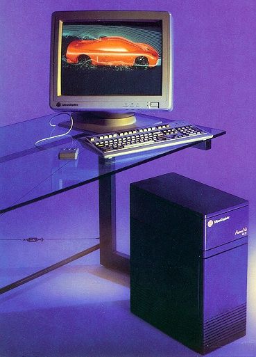
IrisVision is not a product that was intended for PC from the beginning, and most of the chips it contains were not designed specifically for it. Its history was more complicated. In 1988, SGI introduced a “low-cost” 3D graphics UNIX workstation called Personal IRIS and that was a big deal. The price for an entry 4D/20 configuration with 8MB of RAM, 8-bit graphics (256 colors) and a 14-inch color monitor was just $13.500. A better equipped configuration with a faster CPU (4D/25), 24-bit graphics (16 million colors), Z-Buffer, 380MB hard drive and 19-inch color monitor cost $34.000 (plus $7000 for a Turbo graphics option that accelerated 20 thousand triangles per second instead of five thousand with the standard graphics).
This might not sound cheap until you compared the prices to 3D hi-end solutions that cost several hundred thousand dollars. The Personal Iris was “cheap” and compact enough to serve as a hi-end personal workstation for demanding 3D graphics tasks.
Silicon Graphics Inc. Personal IRIS (promo photo)
Although SGI’s share in the UNIX workstation market was in single-digit numbers, if you focused just on 3D workstations, SGI sold (annually) as many computers as all its competitors combined. This was not just about the hardware. SGI created a very fast and easy to use 3D API (application programming interface) called IRIS GL (or just GL) which contributed to the success SGI had back then.
IBM made a deal with SGI and licensed both the 3D hardware and IRIS GL API for their then-new RS/6000 line of UNIX workstations. The MCA version of the IrisVision is basically a result of this deal because it uses the same 3D graphics architecture as the Personal IRIS. “The Very Unofficial IrisVision Home Page” says that during the development/testing phase of the product, SGI used IBM PS/2 Model 70 computers to run diagnostic and test programs. PS/2 computers (mostly) had MCA bus just like RS/6000. They were way more affordable and allowed easier direct access to the hardware, so they were ideal for this purpose. Somebody later realized that the card could be offered for IBM PS/2 too, so a VGA pass-through connector was added.
A high-end 25-MHz 386 IBM PS/2 Model 70 computer with the IrisVision installed in the full configuration (24-bit frame buffer + Z-Buffer). A floating-point co-processor is required in order to run IRIS GL programs.
The IrisVision is not compatible with VGA or any other PC graphics standard, so it does not work in the BIOS environment or the DOS prompt. A VGA input connector is used for connecting the IrisVision with a VGA-compatible adapter. Both, the MCA and ISA/AT versions use an external pass-through cable and some logic to pass-through the output from a VGA card to the monitor (connected to the IrisVision) until an IrisVision driver activates its own output in a supported program (unlike with 8514/A, there is no MCA bus AVE extension). Thanks to this, you can use VGA and the IrisVision in a single-monitor setup (a dual-monitor setup is possible too). It works the same way as 3Dfx Voodoo Graphics and Voodoo2 cards.
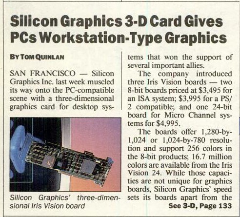
IrisVision made its way to the Infoworld title page (November 5, 1990)
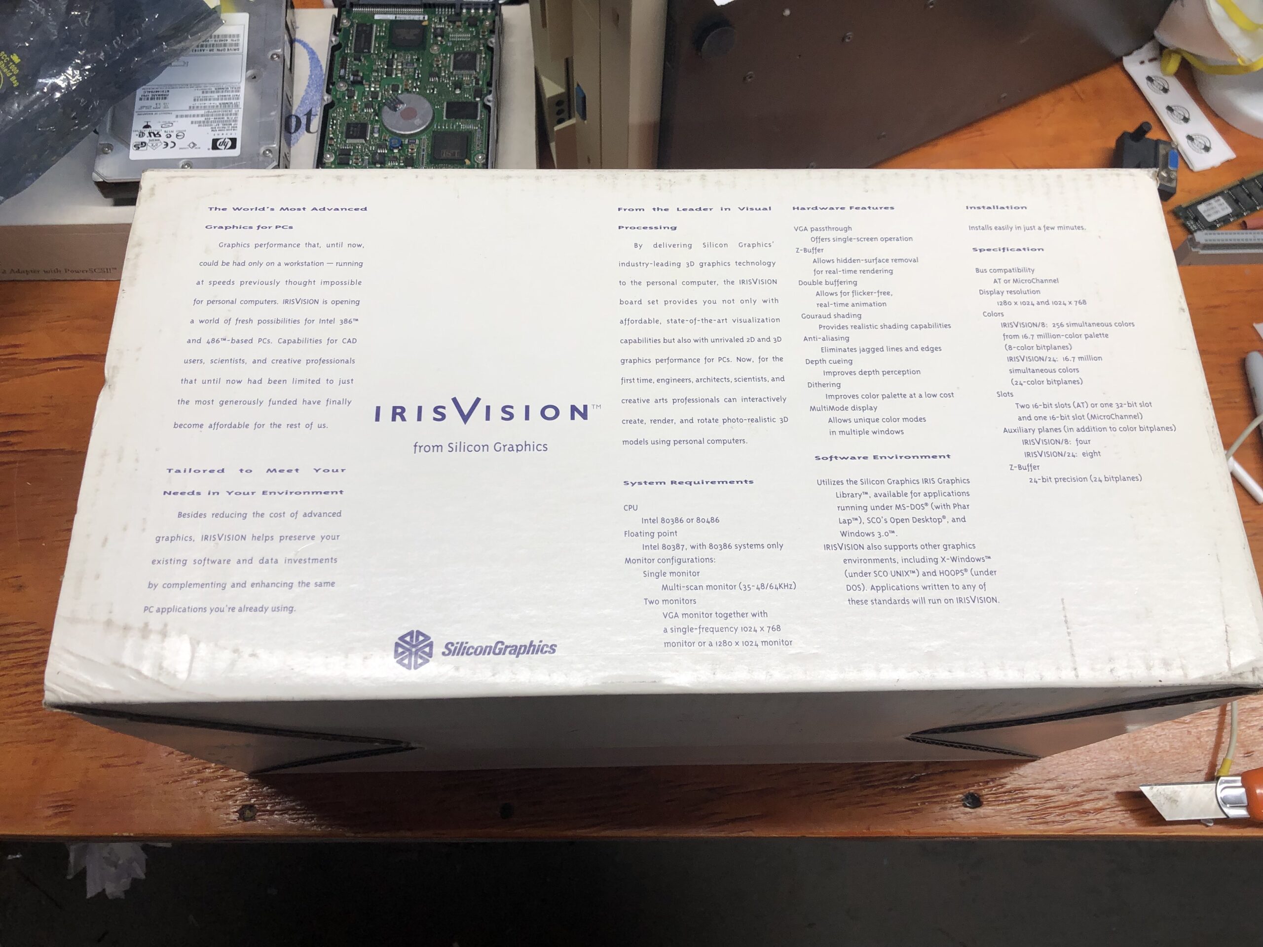
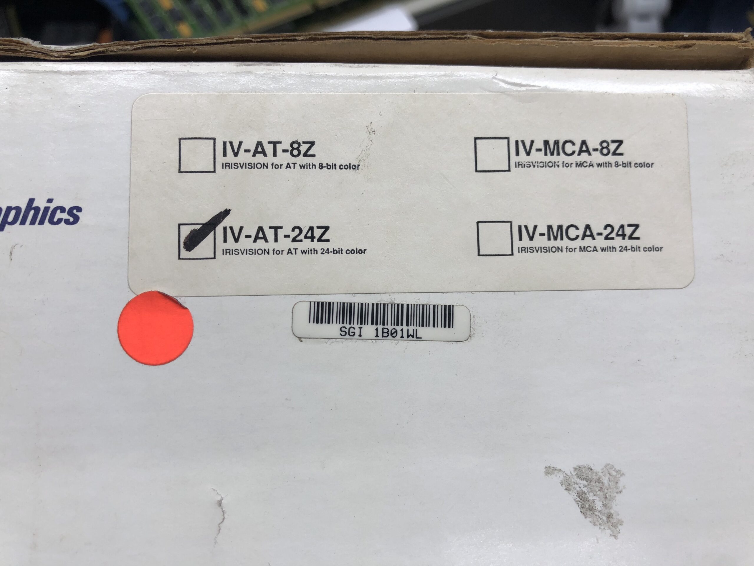
The IrisVision was released for PC and PS/2 in 1990. The MCA and ISA/AT versions are very similar in architecture. The difference is in an additional chip for handling the MCA bus communication and a different monitor output (the ISA/AT version has a standard 15-pin VGA instead of a 3W3 typical for RS/6000 computers). By the end of 1990, prices were the following:
- ISA/AT 8-bit = $3,495
- MCA 8-bit = $3,995
- MCA 24-bit = $4,995
Sadly, it was not specified if a Z-Buffer memory board was included or not (at least later in the lifecycle, all retail versions were equipped with the Z-Buffer board, but I know for sure that some cards were sold without it – maybe those were direct configure-to-order configurations from IBM, who knows…). An SGI press release compared the performance to a Personal IRIS workstation configuration that cost $13,500 at that time (January 1991). However, that might not be entirely true – although the main chips were the same in both solutions, SGI claimed that the IrisVision’s geometry performance was 14 thousand triangles per second. That is 30% lower compared to the Personal IRIS. Maybe the chips were underclocked to ensure that the card cannot overheat in a standard PC, but there is also a chance that SGI just changed the benchmarking parameters (triangle size, flat/Gouraud sharing, Z-Buffer …), so the numbers are not directly comparable.
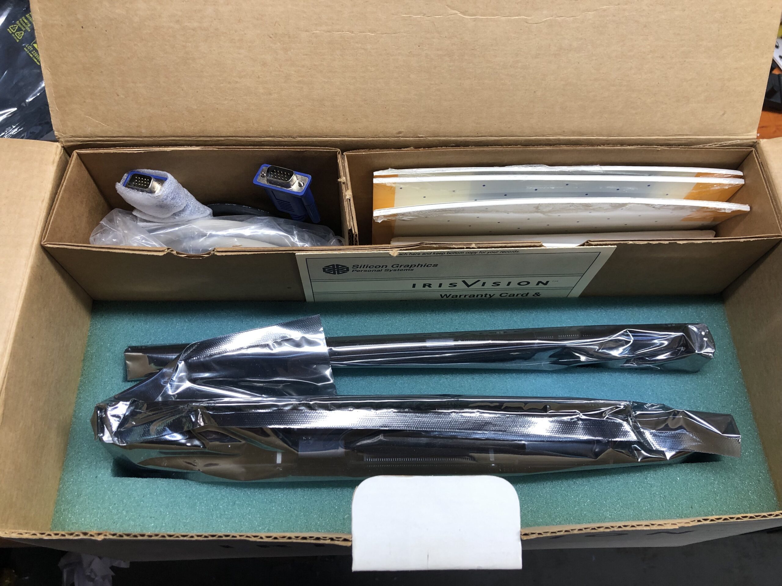
IrisVision original package
Some may think that this was the first true 3D accelerator available for PC, but that’s not true. At that time, there were other more or less successful products, mainly oriented on 3D CAD. The first 3D accelerators for PC were available in the mid-80s. As far as I know, the oldest among the true real-time 3D accelerators is Matrox SM-640 / SM-1281 from 1988 (real-time means the support for double-buffering). These cards provided hardware geometry acceleration (through a licensed SGI chip), a “TIGA” rasterizer, 256 colors, smooth shading and (some say) even a Z-Buffer. It cost $6,995 at the end of 1988.

Matrox SM-1281 in action. A research team used it for accelerating their custom-built VR environment.
If you know any older real-time 3D accelerator for PC, please let me know (Matrox PG-series cards and IBM PGC do not support double-buffering).
Hercules Superstation 3D from 1991 uses a TMS34020 “TIGA” rasterizer combined with an Intel i860 for geometry and lighting calculations. The price was between $4,500 and $5,900. Hercules claimed performance about 20 thousand triangles per second.
Complete 3D acceleration with very little CPU overhead
Feature-wise, the IrisVision is an extremely simple 3D accelerator. It can compute geometry & lighting and draw lines (with optional anti-aliasing), smooth-shaded polygons and stipple-alpha patterns. There is no support for true alpha-blending, fog effect or texturing (which is hardly surprising for chips from 1988). On the other side, all the supported features are fully hardware accelerated with very little use of a host CPU.
This is a simplified overview of what is necessary to do to draw a triangle in a primitive 3D pipeline of an accelerator that does not support alpha-blending or texturing (the text was borrowed from the article about S3 Virge and modified to match this card):
- Geometry transformation: 3D world X/Y/Z coordinates of the vertices (defining a triangle) are transformed into a 2D X’/Y’/(Z’) projection on a screen (based on the camera position & angle in the 3D scene). X’ and Y’ define 2D position on the screen and the optional Z’ defines distance between the camera and the vertex).
- Optional vertex lighting: Colors are calculated for each of the three vertices of the triangle (based on positions of spot/ambient lights in the 3D scene and object material parameters).
- Edge-slope calculations: Slope parameters are calculated for each dimension of each edge (X’/Y’/Z’) of the triangle.
- Edge interpolation: The triangle is decomposed into spans (one-pixel-thin horizontal lines). Based on the vertex positions and already calculated slope parameters of edges between them, edge interpolation is used to define start and end X’/Y’/Z’ positions of each span on the screen.
- Span-slope calculations: Edge-slope parameters are used to calculate R/G/B (color) values for the starting point and slopes between the start and end of each span.
- Span interpolation: Spans are now drawn into framebuffer memory (color buffer and Z-buffer). R/G/B parameters for each pixel are interpolated based on the previously calculated span-slope parameters. If Z (depth) testing is involved and the Z’ value of a new pixel is higher than the Z’ value of a previously stored one (with the same X’ and Y’), drawing of the new pixel can be completely skipped (Z testing conditions can be changed freely, but “less or equal” is the most common setup).
Unlike early consumer 3D accelerators in the mid-90s, which usually accelerated only stages 4-6 (or low-end solution like SGI Indy XL8/XL24 which accelerated just the stage 6), IrisVision does all the stages in hardware. As a result, the solution does not rely much on the CPU performance and (ISA, MCA) bus bandwidth.
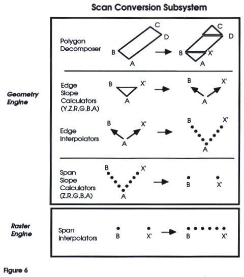
Pipeline stages as shown in SGI manuals
Explaining the graphics architecture – geometry processing
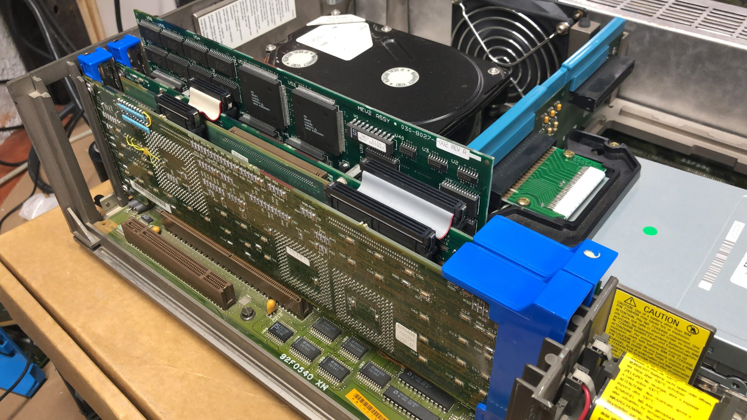
Do not expect that there is just a single GPU chip with some memory and that’s all. Nope. This is from 1988, when the technology was not advanced enough to put all the 3D features on a single chip. That happened almost a decade later. The IrisVision circuits are spread across two full-length boards (ISA or MCA) and up to two additional modules – with everything connected together in a big sandwich.
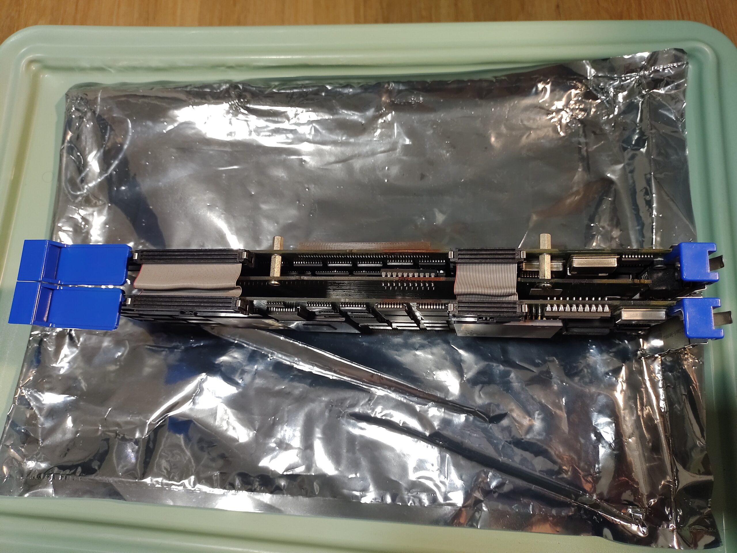
The minimal MCA 256-color configuration wihout a Z-Buffer module
I will go through the MCA boards and explain how the main chips contribute to the 3D rendering handled by the cards:

The front side of the Geometry Engine board (down) and the rear side of the Raster Engine board (up). The brown connector on the Raster Engine Board is used for connecting an optional Z-Buffer module.
All graphics commands enter the Geometry Engine board via the 32-bit MCA bus. That is the card without the monitor output. This is the only way to interact with the card as the other (16-bit) MCA edge connector on the Raster Engine board is used only for power.
The biggest chip on the right side of the board is specific for the MCA version. It handles all MCA specific tasks and provides a bridge to the SGI’s internal bus. The 16-bit ISA version does not need such a chip.
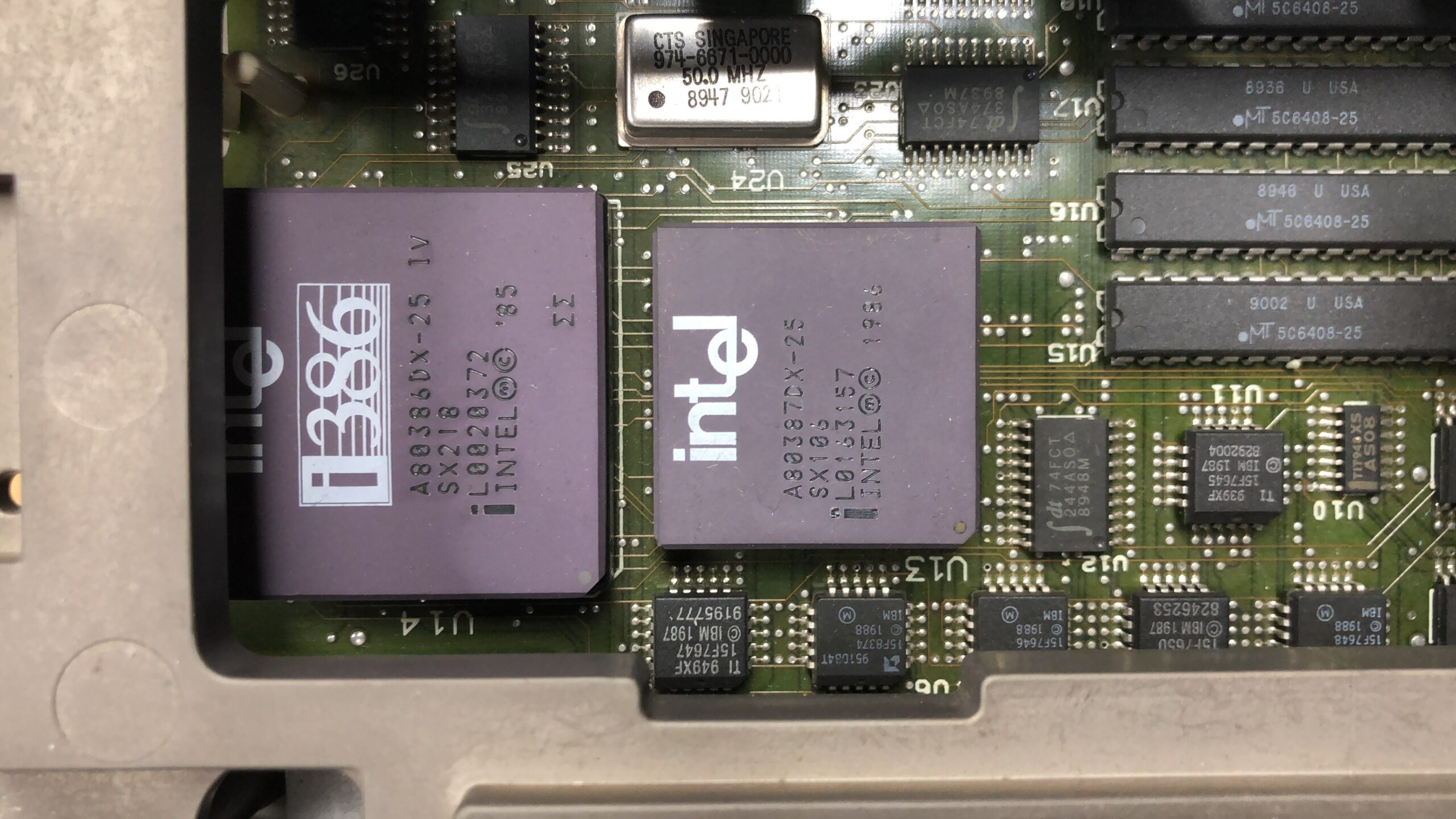
The true heart of this 3D accelerator is a chip called HQ1. It controls the operation of other chips on all boards (both geometry and rasterization). This is in fact a programmable processor with its own memory for a program (160KB, 40-bit bus) and data (32KB, 32-bit bus), working as a microcode sequencer for a floating-point unit. HQ1’s high-speed CMOS static RAM chips are visible on the left side of the card among all the 74-series glue logic chips (buffers etc.). The program memory is located at the column of five CY7C199 chips (32Kx8bit) under the “Silicon Graphics Inc.” text. The data memory is located at the column of four CY7C185 chips (8Kx8bit) right next to it.
The HQ1 calculates geometry and lighting and manipulates with data, so the rasterization part can do its job. However, it supports only integer arithmetic. The geometry is calculated in conjunction with the Weitek XL-3132 32-bit co-processor which is used to off-load all the (single-precision) floating-point commands. The 20-MFlops Weitek chip is just a generic off-the-shelf part, not specifically designed for geometry processing – it just does all the floating-point adds and multiplications requested by the HQ1 for matrix calculations. Both chips run at 10MHz.
All the mentioned chips (together with the GRF1 bus support logic) form a geometry engine. This engine takes care of the first five stages of the 3D pipeline. It decodes IRIS GL commands, converts the 3D space into a 2D projection, calculates vertex color values based on the lights located in the scene (lights are defined by their color, location and direction; objects are defined by surface material properties: ambient, diffuse, shininess…), converts all polygons into single-line spans and sends the span positions together with color and Z slope parameters to the Raster Engine board using a 32-bit communication path in the ribbon cable above the Weitek chip (wireframe lines are drawn directly and not divided into spans).
Raster Engine
The raster engine board has a more straightforward job that does not require powerful general-purpose processors. The biggest challenge here is the required speed. If the speed had not mattered, the raster board would have been more than 50% smaller. The large chip on the left side of the board is the rasterizer itself – the RE2.1. This is the chip that receives the drawing commands from the HQ1 and acts as a pixel generator. All the span or line parameters are stored in its registers and once a draw instruction is sent, it starts iterating X, Y, Z and color values and, based on write masking and write conditioning, it stores the pixels in the memory.
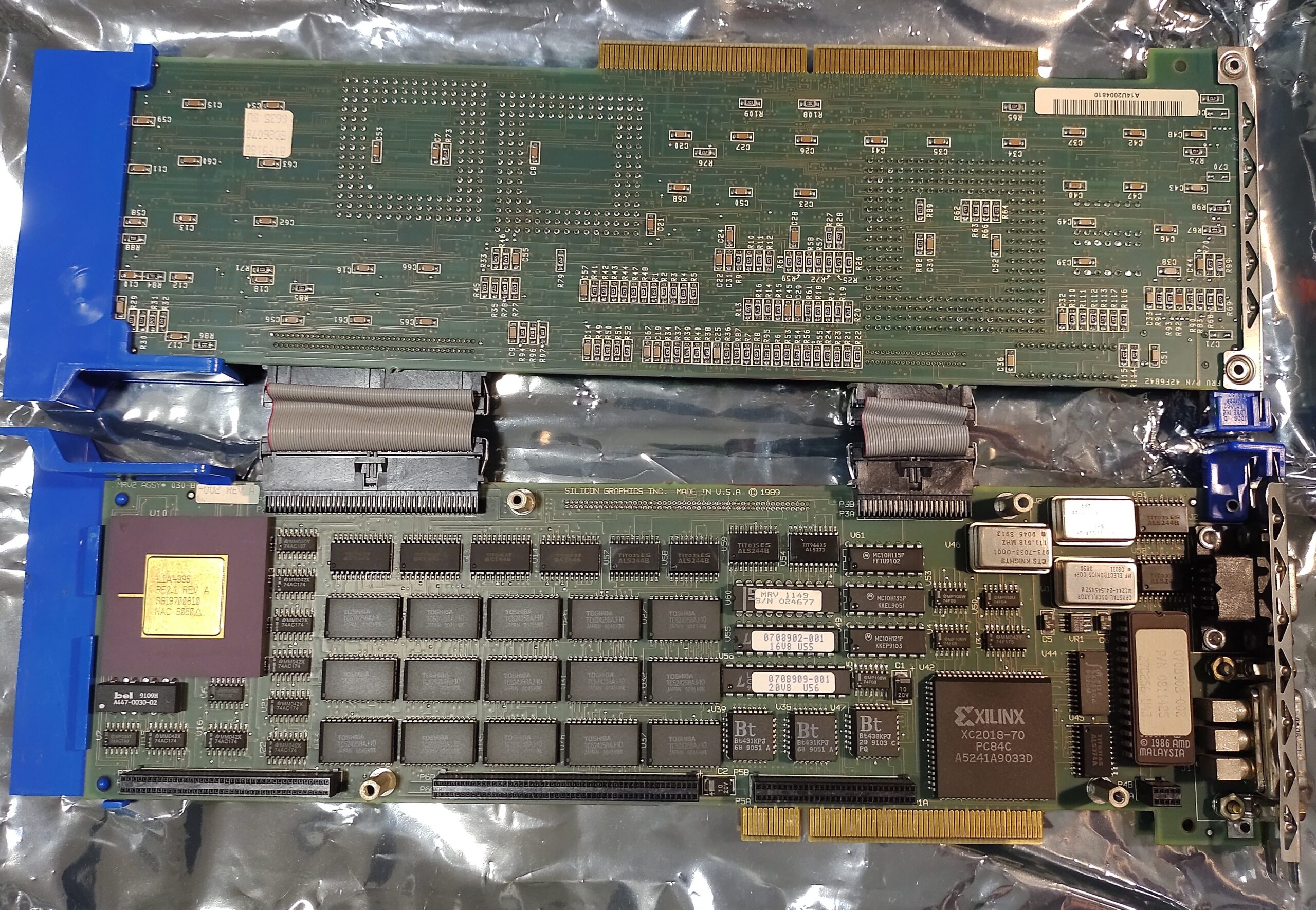
The front side of the Raster Engine board (down) and the rear side of the Geometry Engine board (up)
The whole card supports drawing of the following object according to SGI:
- Points
- Lines and polylines (a series of subsequent lines)
- Filled polygons (flat shaded or Gouraud/smooth shaded)
- Triangle meshes (also called triangle strips)
- Curves and NURBS
- Screen aligned boxes
- Text characters
The RE2.1 rasterizer itself supports just drawing of points, lines (both point sampled and anti-aliased) and spans and it supports bit block transfers with write masks (usable for copying regions from/to/in the framebuffer memory and drawing text characters). Most of the primitives above requires preprocessing from the HQ1 chip: the triangles are split into one-line spans and curves/NURBS are approximated by polylines.
Given the low speed of the memory chips available in the late 1980s, it was necessary to use multiple tricks to get the right performance for the 3D rendering in a resolution of 1280×1024 in up to 256 or 16 million colors. The first trick is to use dual-ported memory chips, so the primary port on each chip can be used for accesses from the RE2.1, while the secondary port is used for sequential reading of the picture data by the display subsystem (controlling the monitor output). These Toshiba TC524258AJ-10 256Kx4bit chips are specifically designed for graphics usage. They also support features like block writes and flash writes to speed up certain operations.
The other trick is a five-way interleaving. If you look again at the rasterizer board, you can see a 5×3 array of these memory chips. In the base configuration, this is the whole memory used to store screen data (1280×1024@8-bit colors). Each column of three chips is always accessed at the same time, so the picture data is stored using 12-bit data path. Such a group of three chips stores 256K of 12-bit words, which means 256×1024 pixels in 12 bitplanes (and all these bitplanes are written at the same time). Having five groups means that the card can store five times more pixels – 1280×1024. Hence, the memory size is 1.875MB.
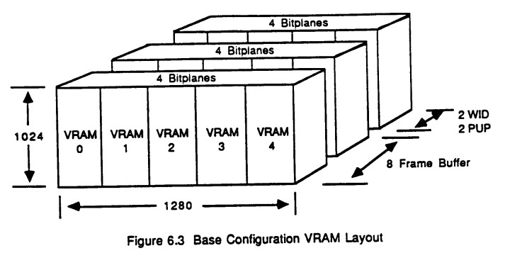
The memory organization of the base 256-color configuration. Every five consecutive pixels are split into all chip groups (VRAM 0-4).
All groups are connected to the same data pins, so the RE2.1 cannot write into multiple groups at the same time. However, the interleaving allows to overcome the long memory access times. Writing a span into the memory means, that every five consecutive pixels are split into all five memory chip groups. When the RE2.1 writes into the first group, the second group is already being prepared for the next write and so on.
If you are wondering why this card has 12 bitplanes when 256 color pixels require just eight bitplanes, the additional four are used for non-color data. SGI designed the original solution for very slow CPUs and wanted to off-load several tasks to the graphics hardware, so the CPU can do other stuff. The four additional bitplanes hold Window ID, overlay and underlay data. The Window ID bitplanes allow the hardware to define multiple 3D viewport windows, so that updating the windows in the background does not overwrite windows that are in front of them. This is used also for context menus that are on top of 3D viewports. The 3D scene rasterizing is bypassed on the pixels that have specific Window ID set. Without this feature, you would need to handle this in software using the main CPU.
Overlay and underlay bitplanes just send information usable for the external video-production equipment doing chroma keying. The card supports genlocking (output synchronization with an external signal) and NTSC timing, so these features made sense back then.
I don’t have my own IrisVision, so I am not able to convert our GPUbench to IRIS GL/DOS (that would not be a difficult task if I had access to the real hardware). However, by analyzing demo recordings provided by an owner (Lorenzo), it seems that the rasterizer performance is ~21 Mpix/s (million pixels per second), so the RE2.1 chip clock might be around 25MHz (but that is just my guess – if you know more, please let me know). This is not very fast, so don’t expect more than single-digit frame rates when the whole screen is covered with filled (or even smooth-shaded) polygons.
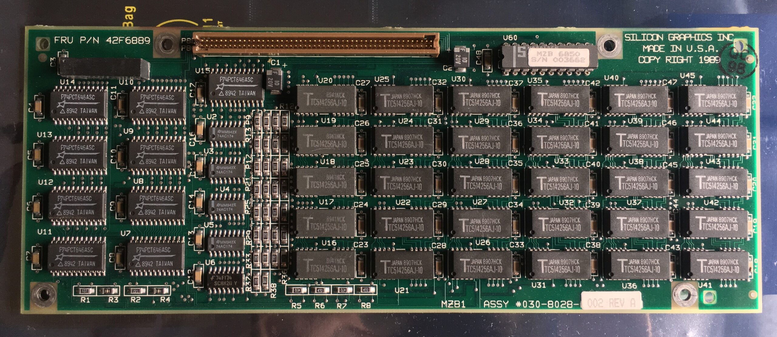
The Z-Buffer option module
The brown connector on the back of the Raster Engine board is used to connect an optional Z-Buffer (MZB) board. The board does not contain any processor as all the depth calculations and hidden surface removal are done by the RE2.1 chip. It just adds the necessary memory. In the photo above, you can see the 6×5 array of Toshiba TC514256AJ-10 DRAM chips (along with 8-bit P74PCT646ASC transceivers and 74AC174 D-type flip-flops). Each chip stores 256Kx4bit of data (128KB), so 30 of them provide 3.75MB (1280×1024, 24 bits per pixel). These chips are simpler than those used for storing color values of pixels as they are not dual-ported. The dual-ported architecture would be useless for the Z-Buffer because its content is not sent further to the display subsystem.
There is again 5-way interleaving like with the color buffer memory. The RE2.1 has separate data pins to get all 24 bits (stored in six memory chips) of a pixel from the Z-Buffer together with the 12 bits of a pixel from the color buffer in a single step. As a result, Z-Buffer accesses do not slow down color buffer accesses.
The Z-Buffer operation is very simple. The RE2.1’s Z-iterator calculates depth value of each new pixel (this value expresses the distance between the pixel and the viewport of the camera) and the value is then compared with the value of the previously drawn pixel at the same screen location (stored in the Z-Buffer). Based on the settings, the drawing operation of the new pixel is skipped if its depth value is higher than the depth value of a pixel previously stored at the same location. Thanks to this feature, a program does not have to spend CPU time sorting all polygons from far to near (and it also allows intersecting objects).
NOTE: I don’t know whether the IrisVision’s driver is able to use software Z-Buffer like low-end graphics options for SGI Indigo and Indy. Their graphics drivers have a Z-Buffer allocated in main memory, compute the depth tests using the CPU and send the results using a 1-bit 32-pixel mask that tells the rasterizer which pixels should be skipped. The IrisVision’s RE2.1 chip have some support for pattern masking too, but I doubt it would be efficient to use it this way. The IRIS GL Programming Guide does not mention any software Z-Buffer option for the Personal IRIS (which shares the same graphics chips), so I assume that the software Z-Buffer is not implemented.
Display Subsystem
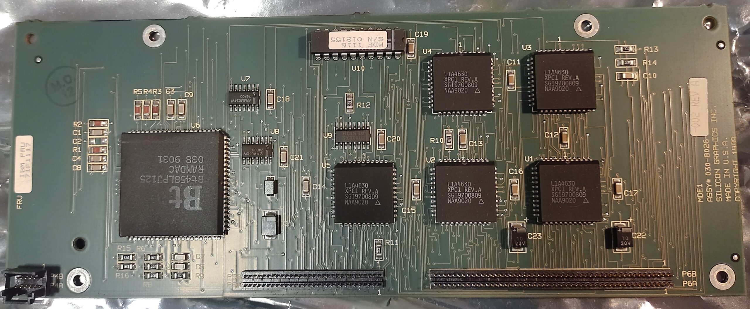
Although the raster board contains the monitor output and pass-thru connectors, the RAMDAC (digital-to-analog converter for signals driving a monitor) is located on a separate board, because there are two choices based on the adapter configuration. The base configuration has a simple module attached to two wide black connectors on the raster board (the one in the middle and the one on the right):
The Raster Engine board again for your convenience
8-bit Frame Buffer Option module
The Xilinx 2018-70 (programable logic array) on the Raster Engine board works as the Display State Machine, orchestrating all display subsystem components to work together. There are three Bt branded chips close to it – two of them are cursor chips (the third one is just a clock generator). Each of these Bt431KPJ cursor chips has internal 1-bit memory for a cursor image with a size of 64×64 pixels. You can use them either separately (for example for two crosshair cursors on independent locations) or together to create a single 2-bit cursor (three colors + transparency).
The second data port of the color buffer memory chips, the outputs from the cursor chips and control signals from the Display State Machine go through the wide black connectors to the module containing five XPC1 chips and a single 256-color RAMDAC (Bt458LPJ125). The XPC1 chips work with the 5-way interleaving, so each is connected to its one fifth of the color buffer memory. Each of the cursor chips has five outputs (thanks to their native support for 5:1 output multiplexing), so they can be connected directly to all XPC1 chips.
Each XPC1 chip combines data from the color buffer memory (pixel color, Window ID, overlay/underlay) and cursor chips and generates an 8-bit formatted pixel color value and a 2-bit overlay value. Thus, no matter how the pixels are stored in the framebuffer memory, after being processed by the XPC1 chips, they are converted into a color index for a 256-color palette. That’s the only format that the RAMDAC accepts here.
The base adapter configuration supports the following pixel formatting (defined per pixel using the Windows ID bit planes):
- Single-buffered 8-bit color-indexed mode (256 colors with a custom color palette)
- Single-buffered 8-bit RGB232 mode (256 colors with a generic RGB palette; red = 2 bits, green = 3 bits, blue = 2 bits)
- Double-buffered 4-bit color-indexed mode (16 colors with a custom color palette)
Both 8-bit modes (color-indexed and RGB) work the same from the hardware point of view. The difference is just in the palette that is loaded in the RAMDAC. In these modes, XPC1 does not do any color conversion. It checks the outputs from the cursor chips and if at least one of them has its output active, it outputs a cursor-colored pixel instead of the original pixel stored in the framebuffer. Cursor chips are synchronized with the rest of the display subsystem, so they know the position of the pixel that is currently being processed, and they can control their output based on stored cursor shapes and X-Y cursor location registers. The cursor drawing handled in hardware is just another feature that helps reducing CPU load.
When a double-buffered 4-bit (16-color) mode is involved, the eight color bitplanes are split into two halves – each half is representing one of the two buffers. Two frame buffers are necessary for real-time 3D, because they allow hiding incomplete frames from a user. While the RE2.1 renders a new frame in one of the buffers, the other one (with contains an already rendered previous frame) is being accessed by the display subsystem and sent to a monitor. When a new frame is complete, the buffers get flipped.
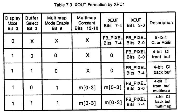
When two 4-bit color values are stored in a single byte in the 16-color double-buffered mode, the XPC1 takes only one half of the byte (nibble) and produces output, where the lower nibble is the color value and the upper nibble is filled with zeros or a user defined “multi-map” constant (being a pointer to the 256-color palette). As a result, a window that uses this double-buffered mode, uses 16 consecutive colors from any of the 16 regions of the 256-color palette. Such a palette is shared with the rest of the screen (drawn in the single-buffered 256-color mode) and cannot be defined independently. This is a big difference between the IrisVision and later low-cost SGI solutions (Indy XL/Newport).
The RAMDAC is the last stage before the picture data are sent to a monitor. The Bt458 allows storing one 256-color palette for standard picture data and one 4-color palette for overlay (each color is defined by the 24-bit RGB888 format). These palettes should be changed only during vertical retrace interval to avoid color artifacts.
The RAMDAC has five pixel-input ports which are connected to all five XPC1 chips and sequentially cycled. The part used in this card has 125MHz pixel clock and the IrisVision allows 1280×1024 in no more than 60Hz (108MHz pixel clock). There were monitors and graphics cards supporting higher refresh rates when the IrisVision was introduced. Being fixed to just 60Hz was not very ergonomic unless you had a CRT screen with medium/long-persistence phosphor.
The card supports following resolutions:
- 1280×1024@60Hz
- 1024×768@60Hz
- NTSC 640×480@59.94Hz interlaced
- PAL 768×576@50Hz interlaced
- 1280×492@120Hz stereoscopic (60Hz for each eye)
The MCA version of the raster engine board has a weird monitor output also used in IBM RT and RS/6000 professional workstations (3W3). The ISA version has a standard VGA connector for both input and output.
The 24-bit Frame Buffer Option
The IrisVision can be expanded to support the 24-bit color mode (16.7 million colors). The more advanced version of the solution replaces the module containing XPC1 chips and the 256-color RAMDAC with a much larger module. The larger module contains array of 5×5 dual-ported memory chips (the same as on the raster engine board) with additional 3.125MB of framebuffer memory. These add 20 bitplanes to be accessed in parallel with 12 bitplanes from the base configuration (so there is no performance decrease with higher color depth). The RE2.1 in the expanded configuration utilizes its full 32-bit data path to the framebuffer (color, window ID, overlay/underlay) and a 24-bit data path to the Z-Buffer.
24 bitplanes of the framebuffer are used to store the color value of a pixel, four bitplanes are used for Windows ID and the remaining four bitplanes are used for overlay/underlay.

24-bit Frame Buffer Option module
The base adapter configuration supports following pixel formatting modes (defined per pixel using the Windows ID bit planes):
- Single-buffered 24-bit direct RGB888 mode (16.8 million colors)
- Double-buffered 12-bit RGB444 mode (4096 colors)
- Double-buffered 12-bit color-indexed mode (4096 with a custom palette)
- Double-buffered 4-bit color-indexed mode (16 colors with a custom color palette)
To allow better color modes, it was necessary to replace both XPC1 chips and the original RAMDAC. XPC1 were replaced with XMAP2 chips, where each XMAP2 also has its own three color-map chips to store a palette of 4096 colors (each represented by a 24-bit RGB value). Although the XMAP2 is heavily extended compared to the XPC1, its core function is the same. It reads pixel data from memory (and cursor chips) and converts them into something that can be understood by a RAMDAC.
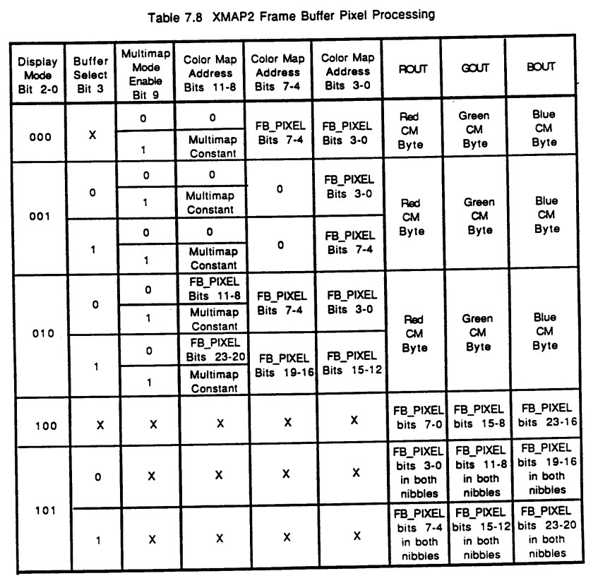
The 24-bit frame buffer option contains three Bt457KPJ125 RAMDACs, where each of them handles one of the color channels (red, green, blue). As a result, unlike the XPC1, the XMAP2 has to output the final color value. It performs color look-up for color-indexed modes and converts the pixel value to the 24-bit RGB888 output. Only the gamma correction is performed in the RAMDACs.
Using the IrisVision in DOS
The MCA version of the IrisVision was designed to run in both IBM RS/6000 and IBM PS/2 computers. The RS/6000 series of UNIX computers ran the IBM AIX (“Advanced Interactive eXecutive”… lol) operating system for which IBM licensed the whole SGI’s IRIS GL library. Thus, it was easy to port GL programs from SGI’s own computers to the RS/6000. The IrisVision was used only as a low-end device in the RS/6000 line. IBM also designed its own hi-end 3D graphics solution that was compatible with IRIS GL (the support for IRIS GL was finally dropped around 1999).
I haven’t found much information regarding using this board set in the RS/6000. The higher chance to find this MCA board set is in a 386 or 486 PS/2 computer. The configuration in DOS is fairly simple – it seems much easier than configuring TIGA graphics cards. The MCA version was provided with an ADF (Adapter Description File), which is required by MCA-based machines to do the initial configuration in the computer’s firmware. The ISA version does not have anything like that, but you must set interrupt level and I/O address range using DIP switches on the Geometry Engine board.
MCA ADF configuration of the card in a PS/2 computer
Once a card is configured in BIOS, you need to run the iv_conf program to set monitor parameters (resolution, sync type, gamma, size and VGA pass-through). The program creates a DOS environment variable called IV_CONFIG in AUTOEXEC.BAT, so other applications can access the user-defined configuration (it is the same concept as with the BLASTER variable used for Sound Blaster audio board configurations).
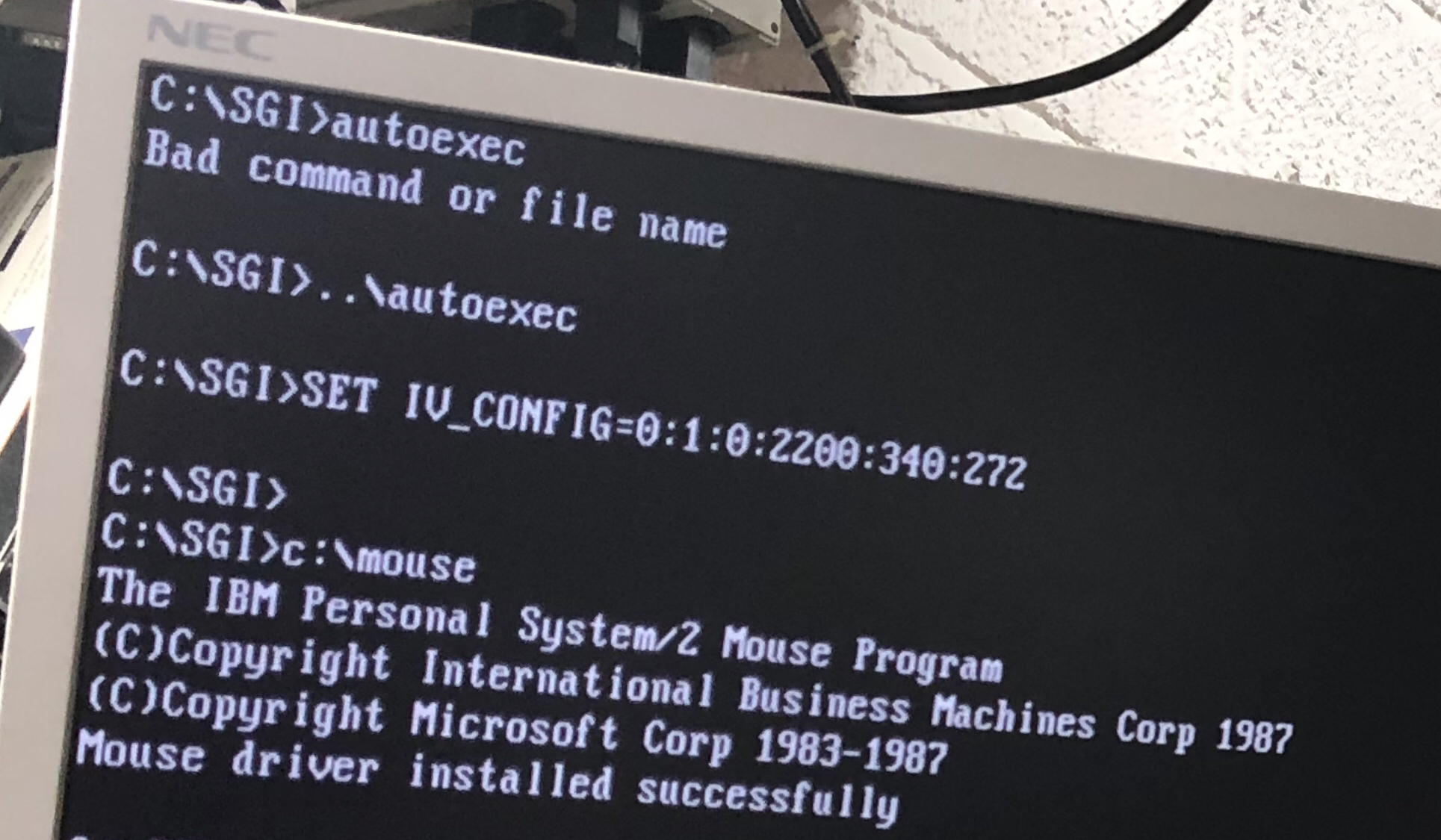
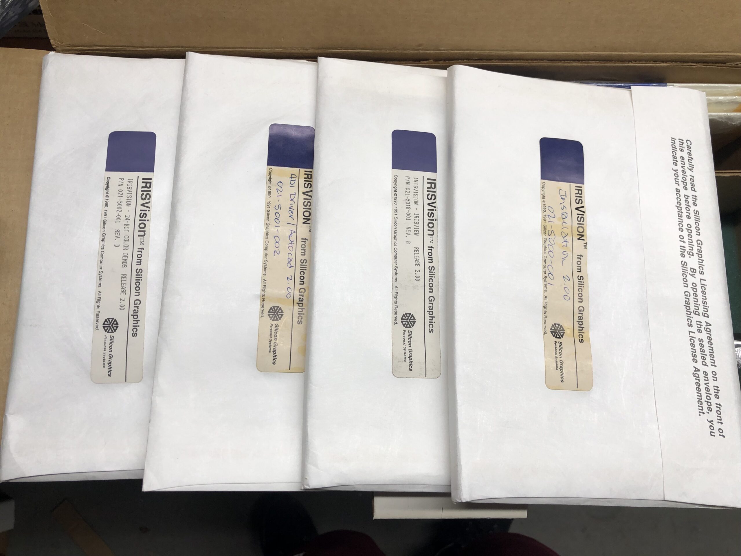
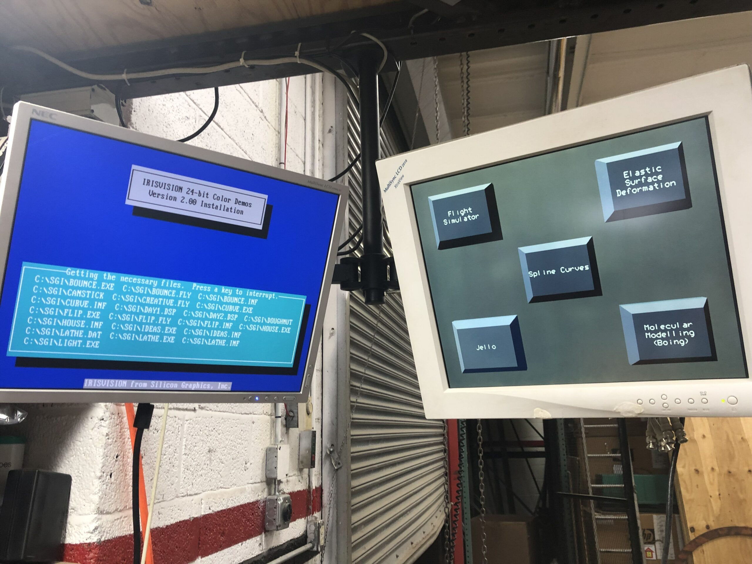
This is all you need in DOS (along with a generic mouse driver) to run IRIS GL programs. The manufacturer ported multiple IRIS GL demos from IRIX and bundled them with drivers and SDK. The most important at that time was the Autodesk ADI Combined Display/Rendering driver that allowed accelerated graphics in programs like AutoCAD (DOS versions), 3D Studio and AutoShade. I looked inside the drivers and it seems that they are not limited just to 2D acceleration functions. They can leverage 3D geometry and rasterization acceleration including anti-aliased lines (the anti-aliasing works only with a 24-bit framebuffer option installed).

Vendor supplied ADI drivers often added new features to AutoCAD. This one is no exception – it adds a “BirdsEye” and “Real-time BirdsEye” features. These allows you to zoom and pan in your drawing. The real-time version window draws in monochrome, but it is double buffered, which allows real-time update as you move the mouse. Like with TIGA and other non-standard graphic cards, the IrisVision can work in the dual monitor mode, where a monitor connected to a standard VGA is dedicated for the AutoCAD’s command console.
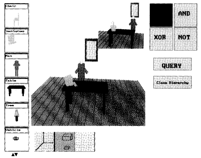
A supplied program called IrisView allows importing DXF files (used by AutoCAD and other CAD programs) and displaying them in real-time 3D. The program lets you configure light sources and render it in higher quality. You can even walk through your 3D scene.
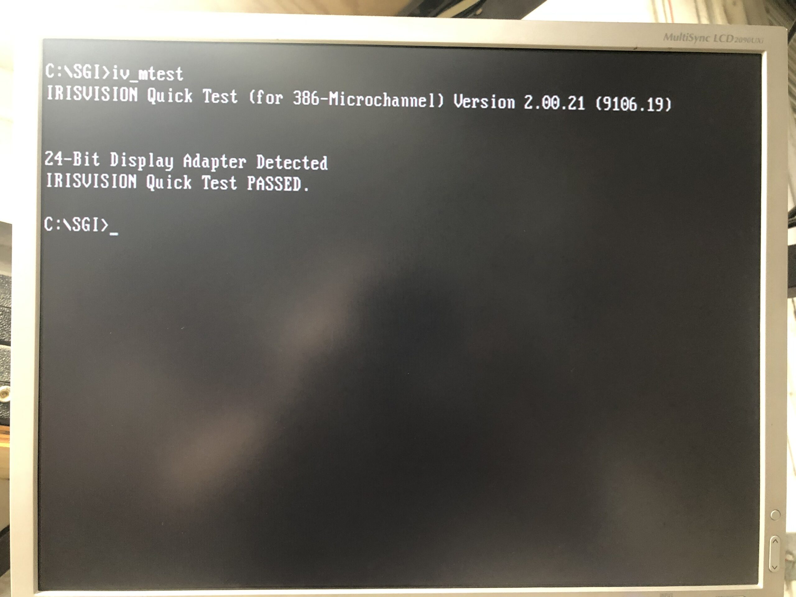
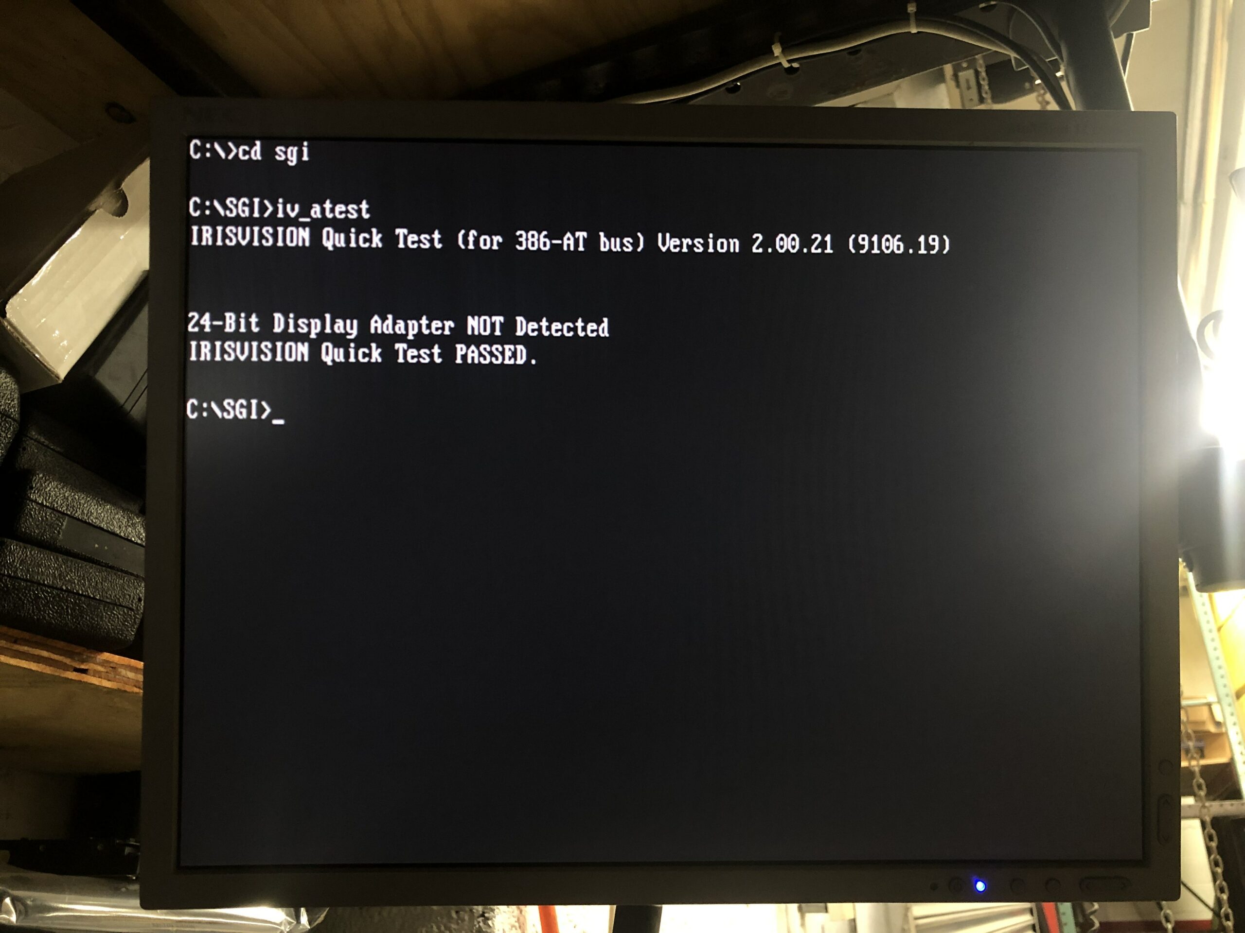
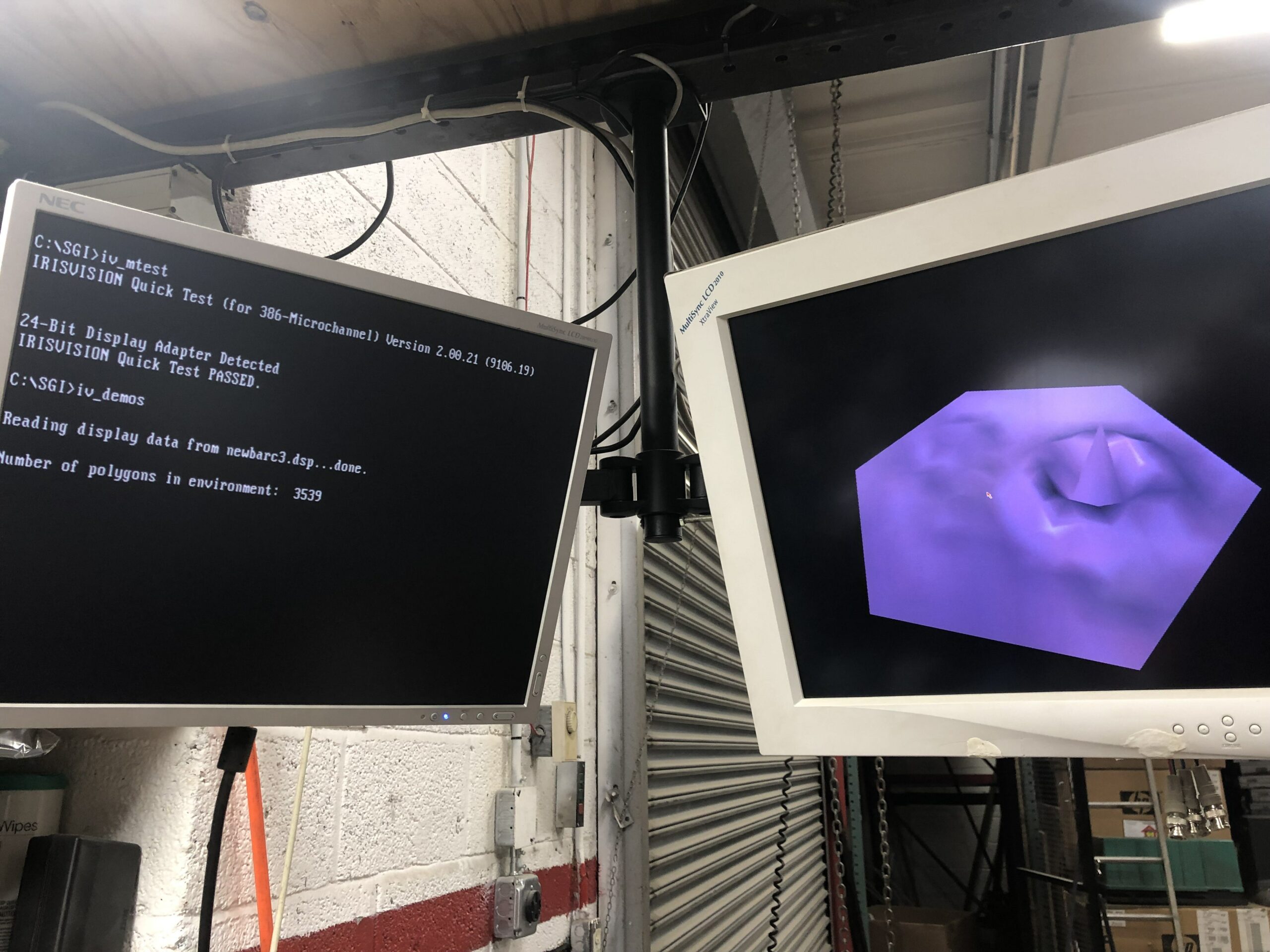
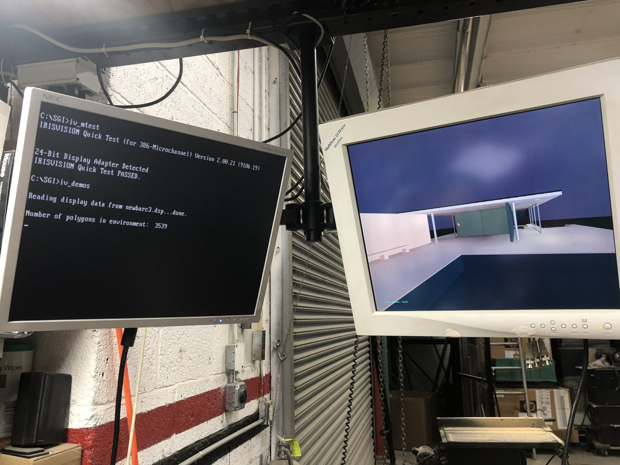
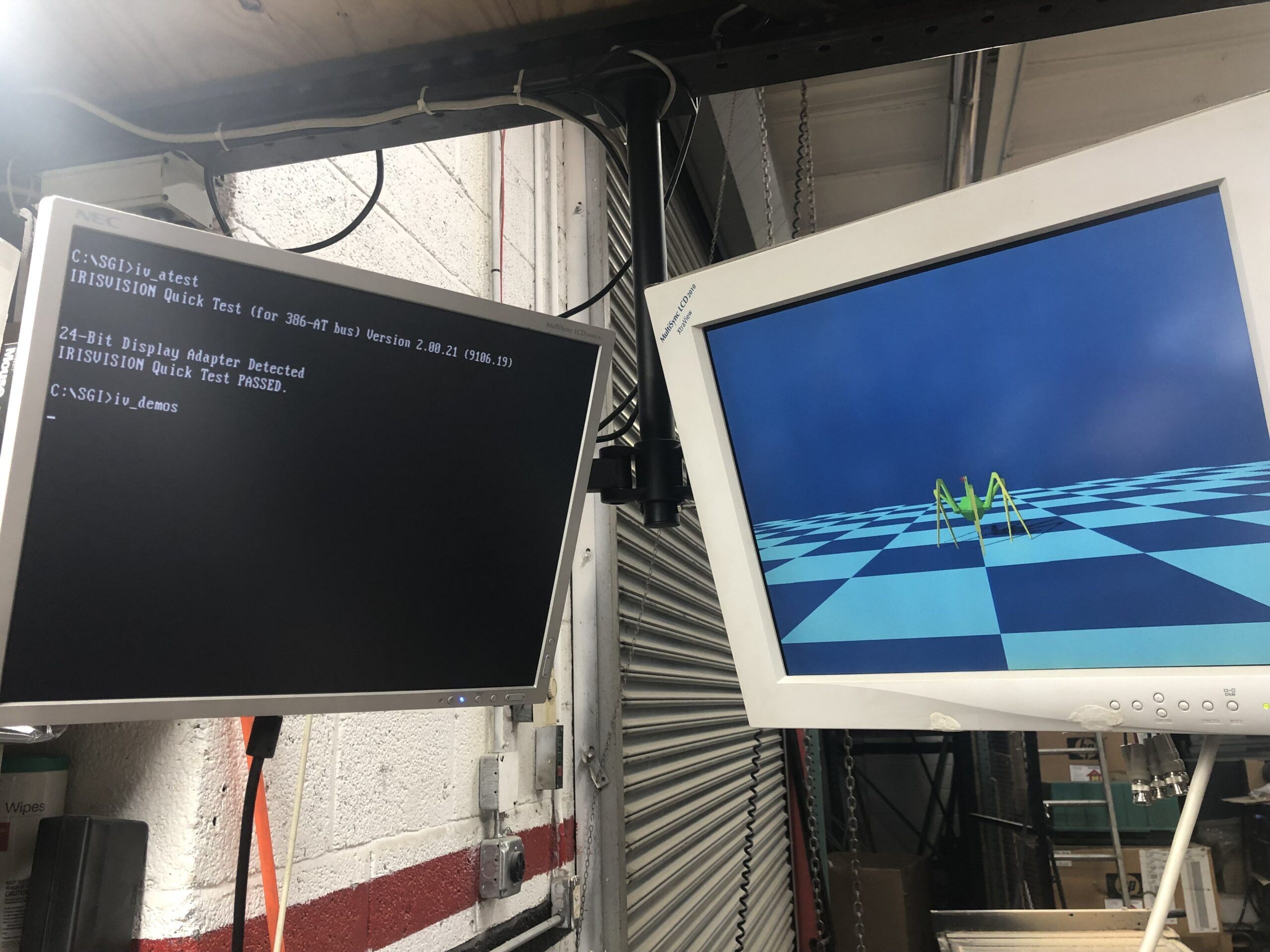
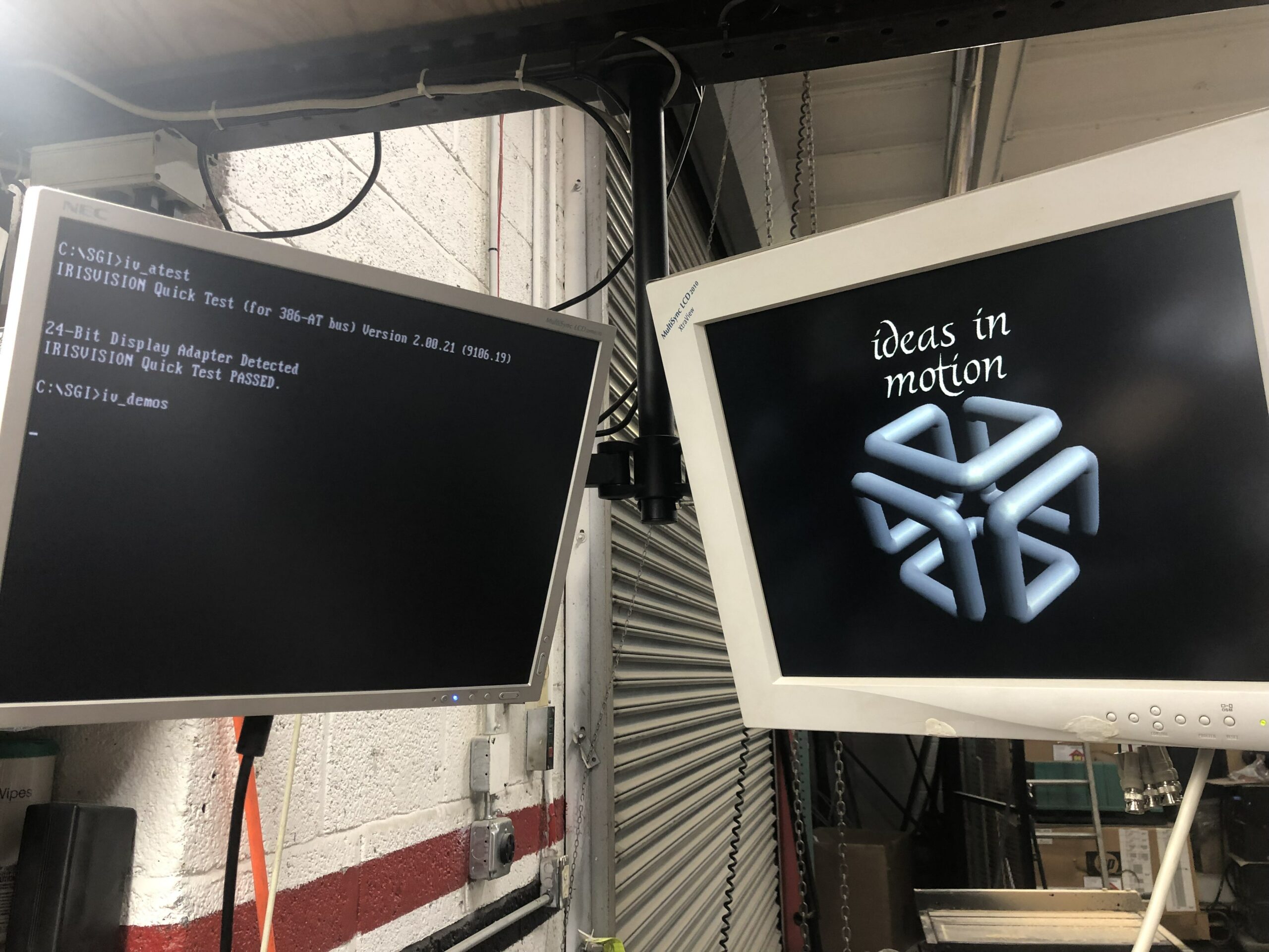
Check the card in action running the bundled demos:
Windows 3.x Drivers
Pellucid made an IrisVision driver for Windows (btw, Pellucid was a short stop for 3Dfx guys after they left SGI and before they started their own company – the world is small). However, the driver is compatible only with the ISA version of the board set. Don’t expect the driver to add any 3D support to Windows. It only allows using the IrisVision as a 2D graphics card for displaying Windows desktop.
A user can select between 1024×768@60Hz and 1280×1024@60Hz. The base configuration uses the color-indexed 256-color mode and acts like any other 256-color adapter under Windows (no Windows ID support or 16-color double-buffering). With the 24-bit frame buffer option installed, you can use the true-color mode with simultaneous 16.7 million colors (the 256-color mode works too if desired).
The driver is not entirely dumb, though. It includes basic 2D acceleration (bit block transfers), so the screen updates should be fast when moving program windows. At least unless you use a desktop background bitmap image – the background redrawing would remind you how slow the 16-bit ISA bus is (3D rendering is less bus-bandwidth demanding than transferring bitmap images from/to the card here).
The lack of a display driver for the MCA version is not a big issue. IRIS GL and ADI-compatible programs are DOS-based anyway and run in full-screen. The Windows 3.x driver was released in 1993, so at that time, you could buy an affordable 2D graphics accelerator with support for higher refresh rates in 1024×768 and 1280×1024 and use it in conjunction with the IrisVision.
The power of IRIS GL
The biggest strength of the IrisVision solution was the IRIS GL support. The DOS implementation was done using the Metaware High-C compiler and the PharLap DOS-extender. If you ever worked with these products, you know how liberating it was to work with them compared to then traditional 16-bit development tools. They were unbelievably fast and the code they could generate was in many cases close to the speed of programs written in assembly. It allowed developers to create true 32-bit protected programs without all the struggle with the conventional memory and segment/offset registers. This created a simple way to take advantage of all the power hidden in Intel 386 (and newer) CPUs.
The development environment was designed the way that made porting of UNIX programs easier. That was useful for SGI and every software vendor who wanted to port their programs from IRIX/AIX to DOS. IRIS GL was also designed to provide windowing functions and other goodies that helped with quick development of complete programs with a user-friendly interface.
The IrisVision was not a successful product in the world of PCs. However, that can be said about nearly all 3D accelerators from that era. That’s why most people today think that the 3D acceleration made its way into PCs half a decade later.
The IrisVision was rather low-cost among available 3D accelerators, but it was still too expensive compared to fast professional 2D accelerators (both fixed-function and programable like TIGA). The other problem was that IrisVision was not very fast, so it did not bring enough attention of software vendors. If you were a typical CAD user during 1992-1993, it made more sense to buy a good professional 2D accelerator and a fast CPU instead of this product. A fast CPU provided benefits in all programs, not just the few supported by the IrisVision drivers. A good 2D accelerator also usually offered more ergonomic refresh rates (at least 75Hz).
Those who really needed 3D bought an SGI UNIX workstation instead – with a much longer list of programs that can utilize the 3D hardware.
Special thanks to Lorenzo Mollicone (ibm@nycellc.com, Instagram: chulofiasco) and George Rudolf Mezzomo who provided me with the photos of the boards. Lorenzo has multiple working board sets and showed me photos/videos of SGI demos and OS configuration, which helped me to better understand how the IrisVision works.
Great article! A have an IrisVision set (24-bit without the Z-buffer option) running in my PS/2 95A. I managed to get the MetaWare compiler required for the SDK and succeeded in compiling some IrisGL examples, will have to put it online some day.
Nice reading: I once bought a MCA with Z-buffer board set at a flea market for a few euros that I could never test it since I do not have an MCA system.
Thank you for your intensive writing about SGI IrisVision add-in. It’s really helpful to understand the change of computer industry in 90s.